- 您现在的位置:买卖IC网 > Sheet目录489 > NTHD4508NT1G (ON Semiconductor)MOSFET 2N-CH 20V 3.1A CHIPFET
�� �
�
�NTHD4508N�
�Power� MOSFET�
�20� V,� 4.1� A,� Dual� N?Channel� ChipFET� t�
�Features�
�?� Low� R� DS(on)� and� Fast� Switching� Speed�
�?� Leadless� ChipFET� Package� has� 40%� Smaller� Footprint� than� TSOP?6�
�?� Excellent� Thermal� Capabilities� Where� Heat� Transfer� is� Required�
�?� Pb?Free� Package� is� Available�
�Applications�
�?� DC?DC� Buck/Boost� Converters�
�?� Battery� and� Low� Side� Switching� in� Portable� Equipment� Such� as� MP3�
�Players,� Cell� Phones,� DSCs� and� PDAs�
�?� Level� Shifting�
�V� (BR)DSS�
�20� V�
�http://onsemi.com�
�R� DS(on)� TYP�
�60� m� W� @� 4.5� V�
�80� m� W� @� 2.5� V�
�D� 1� ,� D� 2�
�I� D� MAX�
�4.1� A�
�MAXIMUM� RATINGS� (T� J� =� 25� °� C� unless� otherwise� noted)�
�Parameter�
�Drain?to?Source� Voltage�
�Gate?to?Source� Voltage�
�Symbol�
�V� DSS�
�V� GS�
�Value�
�20�
�±� 12�
�Unit�
�V�
�V�
�G� 1� ,� G� 2�
�Continuous� Drain�
�Current�
�Power� Dissipation�
�Steady�
�State�
�t� v� 5s�
�Steady�
�T� J� =� 25� °� C�
�T� J� =� 85� °� C�
�T� J� =� 25� °� C�
�T� J� =� 25� °� C�
�I� D�
�P� D�
�3.0�
�2.2�
�4.1�
�1.13�
�A�
�W�
�S� 1� ,� S� 2�
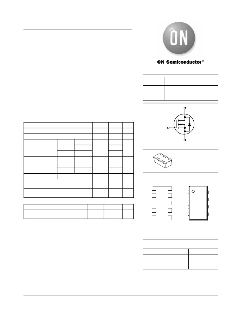
�N?Channel� MOSFET�
�ChipFET�
�CASE� 1206A�
�State�
�t� v� 5s�
�T� J� =� 85� °� C�
�T� J� =� 25� °� C�
�0.59�
�2.1�
�STYLE� 2�
�Pulsed� Drain� Current� t� p� =� 10� μ� s�
�Operating� Junction� and� Storage� Temperature�
�I� DM�
�T� J� ,�
�T� STG�
�12�
�?55� to�
�150�
�A�
�°� C�
�PIN�
�CONNECTIONS�
�MARKING�
�DIAGRAM�
�Lead� Temperature� for� Soldering� Purposes�
�(1/8”� from� case� for� 10� s)�
�T� L�
�260�
�°� C�
�D� 1� 8�
�1� S� 1�
�1�
�8�
�THERMAL� RESISTANCE� RATINGS�
�D� 1� 7�
�2� G� 1�
�2�
�7�
�Parameter�
�Junction?to?Ambient� –� Steady� State�
�(Note� 1)�
�Symbol�
�R� θ� JA�
�Max�
�110�
�Unit�
�°� C/W�
�D� 2� 6�
�D� 2� 5�
�3� S� 2�
�4� G� 2�
�3�
�4�
�6�
�5�
�Maximum� ratings� are� those� values� beyond� which� device� damage� can� occur.�
�Maximum� ratings� applied� to� the� device� are� individual� stress� limit� values� (not�
�normal� operating� conditions)� and� are� not� valid� simultaneously.� If� these� limits� are�
�exceeded,� device� functional� operation� is� not� implied,� damage� may� occur� and�
�reliability� may� be� affected.�
�1.� Surface� Mounted� on� FR4� Board� using� 1� in� sq� pad� size� (Cu� area� =� 1.27� in� sq�
�[1� oz]� including� traces).�
�C8� =� Specific� Device� Code�
�M� =� Month� Code�
�ORDERING� INFORMATION�
�Device�
�NTHD4508NT1�
�NTHD4508NT1G�
�Package�
�ChipFET�
�ChipFET�
�(Pb?Free)�
�Shipping� ?�
�3000/Tape� &� Reel�
�3000/Tape� &� Reel�
�?For� information� on� tape� and� reel� specifications,�
�including� part� orientation� and� tape� sizes,� please�
�refer� to� our� Tape� and� Reel� Packaging� Specification�
�Brochure,� BRD8011/D.�
�?� Semiconductor� Components� Industries,� LLC,� 2004�
�October,� 2004� ?� Rev.� 3�
�1�
�Publication� Order� Number:�
�NTHD4508N/D�
�发布紧急采购,3分钟左右您将得到回复。
相关PDF资料
NTHD4N02FT1G
MOSFET N-CH 20V 2.9A CHIPFET
NTHD4P02FT1G
MOSFET P-CH 20V 2.2A CHIPFET
NTHD5903T1G
MOSFET PWR P-CH DUAL20V CHIPFET
NTHD5904NT1G
MOSFET N-CHAN 3.3A 20V CHIPFET
NTHS2101PT1
MOSFET P-CH 8V 5.4A CHIPFET
NTHS4101PT1G
MOSFET P-CH 20V 4.8A CHIPFET
NTHS4166NT1G
MOSFET N-CH 30V 4.9A CHIPFET
NTHS4501NT1G
MOSFET N-CH 30V 4.9A CHIPFET
相关代理商/技术参数
NTHD4N02
制造商:ONSEMI 制造商全称:ON Semiconductor 功能描述:Typical Uses for FETKY Devices
NTHD4N02F
制造商:ONSEMI 制造商全称:ON Semiconductor 功能描述:Power MOSFET and Schottky Diode
NTHD4N02FT1
功能描述:MOSFET 20V 3.9A N-Channel RoHS:否 制造商:STMicroelectronics 晶体管极性:N-Channel 汲极/源极击穿电压:650 V 闸/源击穿电压:25 V 漏极连续电流:130 A 电阻汲极/源极 RDS(导通):0.014 Ohms 配置:Single 最大工作温度: 安装风格:Through Hole 封装 / 箱体:Max247 封装:Tube
NTHD4N02FT1G
功能描述:MOSFET 20V 3.9A N-Channel w/3.7A Schottky RoHS:否 制造商:STMicroelectronics 晶体管极性:N-Channel 汲极/源极击穿电压:650 V 闸/源击穿电压:25 V 漏极连续电流:130 A 电阻汲极/源极 RDS(导通):0.014 Ohms 配置:Single 最大工作温度: 安装风格:Through Hole 封装 / 箱体:Max247 封装:Tube
NTHD4P02
制造商:ONSEMI 制造商全称:ON Semiconductor 功能描述:Typical Uses for FETKY Devices
NTHD4P02F
制造商:ONSEMI 制造商全称:ON Semiconductor 功能描述:Power MOSFET and Schottky Diode
NTHD4P02F_05
制造商:ONSEMI 制造商全称:ON Semiconductor 功能描述:Power MOSFET and Schottky Diode
NTHD4P02FT1
功能描述:MOSFET -20V -3A P-Channel RoHS:否 制造商:STMicroelectronics 晶体管极性:N-Channel 汲极/源极击穿电压:650 V 闸/源击穿电压:25 V 漏极连续电流:130 A 电阻汲极/源极 RDS(导通):0.014 Ohms 配置:Single 最大工作温度: 安装风格:Through Hole 封装 / 箱体:Max247 封装:Tube